切削、研磨、接合
Cutting, Grinding and Bonding
半導体集積回路ではウェハー上に同時に多くの回路を形成し、その回路を個々に分割してチップとしてパッケージに搭載する。この個々に分割することをダイシングと云い、分割する手段として、ダイシングソーによる切断もあるが、ウェハー表面に溝をつけ(スクライビング)て割ることが行われている。分割されたチップを一つ一つパッケージ基板に張り付けるのがダイボンダーである。集積回路の製造過程で工程を重ねるに際し、表面の平坦化を図るためにCMP(化学機械研磨)が使われる。
In semiconductor integrated circuits, many circuits are formed on a wafer at the same time, and then the circuits are divided into individual pieces and mounted as chips in a package. This process is called "dicing," and although dicing saws can be used to cut the circuits, the wafer surface is often scribed to divide them. The die bonder attaches the divided chips one by one to the package substrate. Chemical Mechanical Polishing (CMP) is used to planarize the surface of the wafers in the process of manufacturing integrated circuits.
接合・貼り付け・ダイボンダ
Bonding, Attachment and Die Bonding
半導体ウェハー同士の直接接合には「拡散接合」と「常温接合」がある。前者は基板を密着させ圧力と熱を加えることにより、接合面で原子の拡散が起こり接合される。後者は高真空中で接合する基板表面にイオンビームなどをあてダングリングボンドを形成し活性化することで、常温で強固な接合が得られる。また、シリコン基板とシリコンの熱膨張係数が近いガラスを接合する方法として「陽極接合」という方式がある。ダイボンダは、リードフレームやICパッケージの基板部にICチップを設置ボンディングする装置である。
There are two types of direct bonding between semiconductor wafers: diffusion bonding and room temperature bonding. In the former, the substrate is brought into contact with each other and pressure and heat are applied to cause atomic diffusion on the bonding surface, resulting in bonding. In the latter, a strong bond can be obtained at room temperature by applying an ion beam to the surface of the substrate to be bonded in a high vacuum to form and activate a dangling bond. There is also an anodic bonding method for bonding silicon substrates and glass, which has a similar coefficient of thermal expansion to silicon. Die bonder is a device for installing and bonding IC chips to the substrate part of a lead frame or IC package.
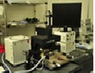
フリップチップボンダー lambda2
Flip chip bonder lambda2
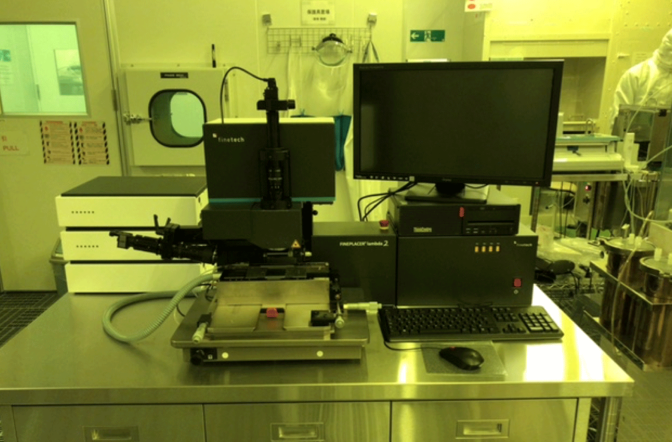
【English】Flip chip bonder lambda2
【別名】FINEPLACER ® lambda2 高精度ダイボンディング、フリップチップボンディング装置
【型式番号】lambda2 finetech社
【apparatus ID】
【機器ID】F-UT-
【機能】国内最強スペックのフリップチップボンダーです。ビームスプリッタを搭載した、ビジョンアライメントシステム(VAS)を搭載。
【Alias】FINEPLACER ® lambda2 High precision die bonding and flip chip bonding equipment
【Model Number】lambda2 finetech
【Apparatus ID】
【Equipment ID】F-UT-
【Specifications】The flip chip bonder with the strongest specifications in Japan. Equipped with Vision Alignment System (VAS) with beam splitter.
マニュアルウエッジボンダ―
Manual wire bonder
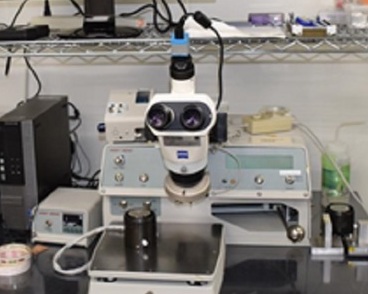
【English】Manual wire bonder
【別名】ワイヤボンダー
【型式番号】WestBond 7476D
【apparatus ID】113
【機器ID】F-UT-126
【機能】アルミ線(または金)
超音波接合
ウエッジ針によって、超音波で配線を刷り込むように接合できる、「何にでもよくつく」ボンダーです。普段は25μmφのアルミ線を常用しています。Zeissの三眼顕微鏡(高精細CCDカメラ付き)により、デバイスの写真や簡単な動画を取得することもできます。
【Alias】
【Model Number】WestBond 7476D
【Apparatus ID】113
【Equipment ID】F-UT-126
【Specifications】Ultrasonic wedge bonding with Al or Au wires. Usually a 25μm diameter Al wire is used. It's possible to acquire nice images or movies thanks to the trinocular microscope Zeiss associated to a high-resolution CCD camera.
エポキシダイボンダ―
Epoxy Die Bonder
【English】Epoxy Die Bonder
【別名】
【型式番号】WestBond 7200C
【apparatus ID】160
【機器ID】F-UT-127
【機能】精密マニュピレータ
銀ペースト接着
実体顕微鏡で斜めから観察しながら、エポキシや銀ペーストでチップを配置することができます。実体は精密マニュピレータですので、その他治具の工夫によって、金バンプの頭を平坦化して揃えたり(コイニング)することも可能です。
【Alias】
【Model Number】WestBond 7200C
【Apparatus ID】160
【Equipment ID】F-UT-127
【Specifications】Precise manipulator. It's possible to look the chip from the side while fixing it with epoxy or silver paste thanks to the stereoscopic microscope.
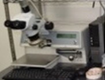
セミオートボールボンダー
Ball bonder
【English】Ball bonder
【別名】
【型式番号】WestBond 4700E
【apparatus ID】143
【機器ID】F-UT-128
【機能】金のボールボンダー
超音波接合
金バンプや、金線によるボールボンディングが可能な装置です。
ディスプレイまたは実体顕微鏡でみながら指定した位置に自動でボールを置いてくれます。
ウェッジボンダ―と比較すると、対象を選びますが、ひとたび条件が出るとこちらの方が安定です。
120μmピッチのLSIチップへのボンディングや、75μmφ金バンプなどで実績があります。
特注の52ピンガラスエポキシピッチ変換基板(金メッキ付)もお分けできます。
【Alias】
【Model Number】WestBond 4700E
【Apparatus ID】143
【Equipment ID】F-UT-128
【Specifications】Ultrasonic ball bonding using gold bump and wires.
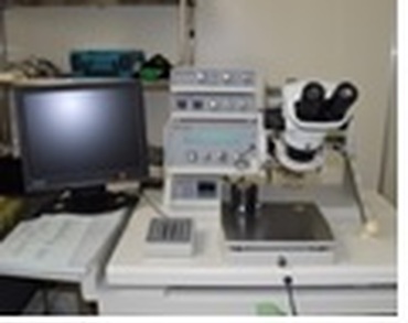
精密フリップチップボンダー
Flip chip bonder
【English】Flip chip bonder
【別名】
【型式番号】Finetech Lambda
【apparatus ID】142
【機器ID】F-UT-129
【機能】ハーフミラーで両方を見ながら位置合わせができる 、このクラスでは「世界最強」のマニュアルフリップチップボンダーです。
手動(マイクロメータによる位置合わせ)精度±0.5μm、角度合わせはアナログ式1ミリラジアン。
チップサイズ15mmまで(治具作成可能)
ランプ加熱による400度熱接合 (超音波オプション購入すれば可能)
【Alias】
【Model Number】Finetech Lambda
【Apparatus ID】142
【Equipment ID】F-UT-129
【Specifications】The chip is aligned with the substrate using a half mirror. Top class manual flip chip bonder with an alignment precision of ±0.5μm in X and Y direction and 1mrad in rotation. Maximum chip size is 15mm. Possible to heat up to 400°C.
ダイシング、スクライバ
Dicing, Scriber
ダイシングは半導体のウェハー上に形成された集積回路などを、ダイシングソーでウェハーを切削して切り出し、チップ化する工程。チップの切り出し法としてはスクライバーによりウェハー表面の切断位置を決めて浅い切れ込みの溝を作りウェハーを割る方式がよく使われる。
Dicing is the process of cutting integrated circuits, etc., formed on semiconductor wafers into chips by cutting the wafers with a dicing saw. The most commonly used method for cutting out chips is to use a scriber to determine the cutting position on the wafer surface, create a shallow cutting groove, and split the wafer.
ステルスダイサー
Silicon Stealth Dicing Machine
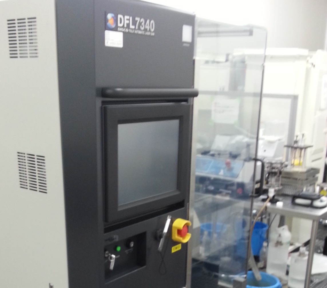
【English】Silicon Stealth Dicing Machine
【別名】ステルスダイシング装置
【型式番号】 DISCO DFL7340(ステルスダイサー・Si用)
【apparatus ID】
【機器ID】F-UT-107
【機能】当拠点のステルスダイサーはシリコン専用ですが、日本発の新技術「ステルスダイシング技術」を利用したダイサーです。
(通常のブレードダイサー:DAD340も公開しています)
レーザー光線をシリコンウエーハの内部に集光することで、意図的に「割れやすい線」を埋め込むことができます。
この線を設計図に従って何本も埋め込み、最後に軽くストレスを与えることで、ウエーハを設計図通りにへき開することができる夢のダイシング装置です。
【Alias】
【Model Number】DISCO DFL7340
【Apparatus ID】
【Equipment ID】F-UT-107
【Specifications】Our stealth dicer is dedicated to silicon, but it is a dicer that uses a new technology from Japan called "stealth dicing technology".
(We also have a regular blade dicer: DAD340)
By focusing a laser beam inside the silicon wafer, it is possible to intentionally embed "breakable lines". By embedding a number of these lines according to the blueprint, and then lightly stressing the wafer at the end, this is a dream dicing machine that can open up the wafer according to the blueprint.
ブレードダイサー
Dicing Saw
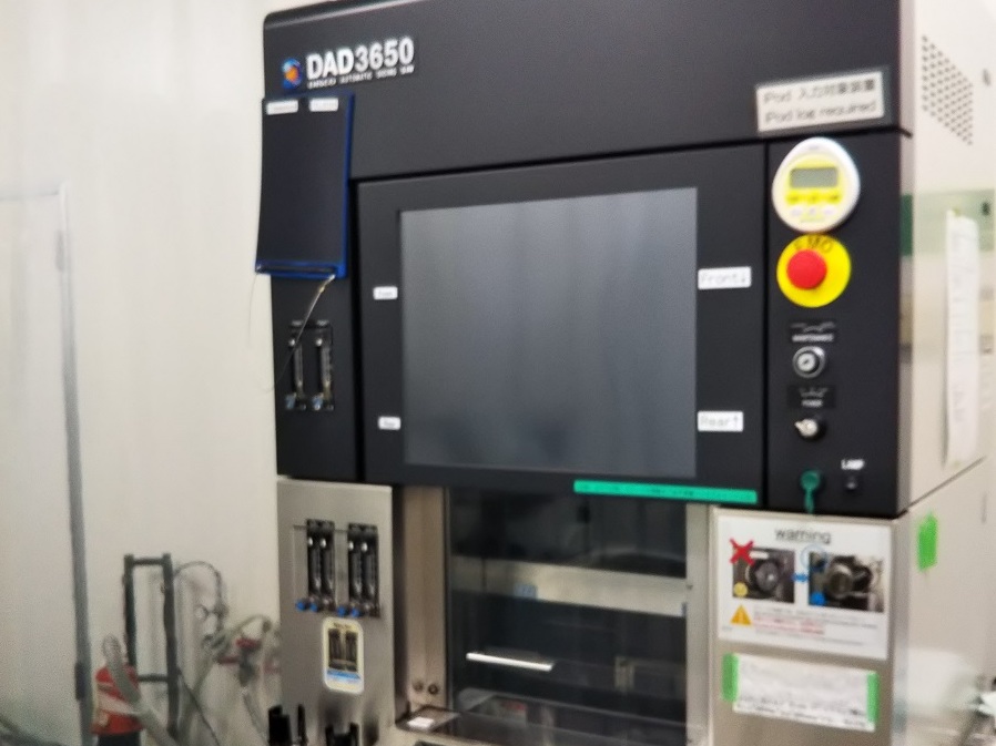
【English】Dicing Saw
【別名】ダイシングソーDAD3650
【型式番号】DISCO DAD3650
【apparatus ID】155
【機器ID】F-UT-144
【機能】二軸スピンドルダイサー
この「二軸機」によれば、四角く切り出したチップ端部を斜めに切りおとすこと(ベベルカット)が可能になり、塗布したレジストの平坦性が担保される効果が期待でき、チッププロセスの収率向上に大きなプラスとなります。
【Alias】
【Model Number】DISCO DAD3650
【Apparatus ID】155
【Equipment ID】F-UT-144
【Specifications】Dual-spindle automatic dicing saw. Bevel cut possible.
CMP(化学機械研磨)
CMP(Chemical Mechanical Polishing)
CMP(Chemical Mechanical Polishing)は、IC製造工程におけるウェーハ表面の平坦化技術の一種で、化学研磨剤、研磨パッドを使用し、化学作用と機械的研磨の複合作用で、ウェーハ表面の凹凸を削って平坦化する装置である。
CMP (Chemical Mechanical Polishing) is a type of wafer surface planarization technology used in the IC manufacturing process. It is a device that uses chemical abrasives and polishing pads to remove unevenness from the wafer surface and planarize it through the combined action of chemical and mechanical polishing.
精密研磨装置
C.M. Polisher
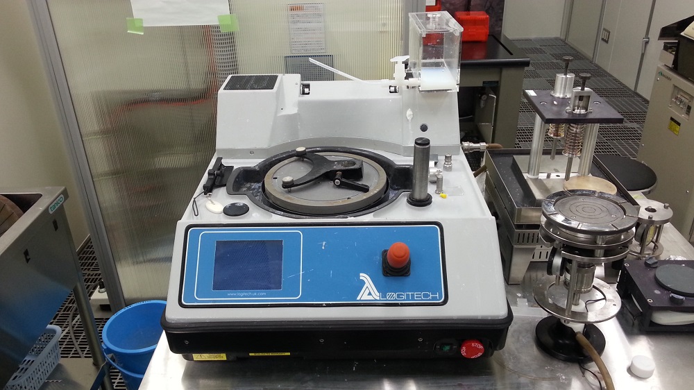
【English】C.M. Polisher
【別名】
【型式番号】Logitech PM5
【apparatus ID】146
【機器ID】F-UT-108
【機能】Logitec 4"化学研磨装置
アルミナの粉によって、対象物を精密に研磨する装置です。
4"丸型ウエーハまで研磨可能。
【Alias】
【Model Number】Logitech PM5
【Apparatus ID】146
【Equipment ID】F-UT-108
【Specifications】Chemical Mechanical lapping and polishing system. Max substrate size: 4''.