リソグラフィ・露光・描画装置
Lithography, exposure and drawing equipment
半導体デバイス等の製作において、微細デバイスや回路の設計パターンをチップ上に形成するために、半導体ウェハー上に塗布したレジスト膜に光によってパターンを焼きこむ描画工程がリソグラフィーであり、その光の露光方式が、パターン精度やスループットに対応して各種ある。また、最近は高価な露光装置を用いない印刷技術(ナノインプリント)や液滴吐出(インクジェット)による簡易な描画技術が開発されている。
In the fabrication of semiconductor devices and other products, lithography is a writing process in which light is used to burn a pattern onto a resist film coated on a semiconductor wafer to form a design pattern for a micro device or circuit on a chip. There are a variety of light exposure methods to meet the pattern accuracy and throughput requirements. Recently, printing technology without using expensive exposure devices (nanoimprinting) and simple writing technology by droplet discharge (inkjet) have been developed.
光露光(マスクアライナ)
Light exposure (mask aligner)
マスクアライナーとは紫外線を用いて試料に微細なパターンを転写・焼付する装置である。一般的にはレジストを塗った試料上にフォトマスクを配置させ、上から紫外線を照射する。露光方式には、密着露光、近接露光(以上コンタクト方式)、レンズを用いた等倍投影露光、縮小投影露光方式がある。また、両面アライメント機能を持ったものもある。
A mask aligner is a device that uses ultraviolet light to transfer and burn fine patterns onto a sample. Generally, a photomask is placed on a resist-coated specimen and irradiated with UV light from above. There are several exposure methods: contact exposure, proximity exposure (or contact method), equal magnification projection exposure using a lens, and reduced projection exposure. Some also have a double-sided alignment function.
光リソグラフィ装置PEM800
Photomask aligner PEM-800
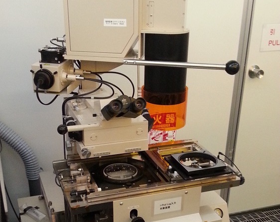
【Eniglish】Photomask aligner PEM-800
【別名】マスクアライナー
【型式番号】UNION PEM800
【apparatus ID】117
【機器ID】F-UT-101
【機能】光によるリソグラフィを行う装置。いわゆる両面5”マスクアライナーと呼ばれる装置です。マスクは5009、4009、2509サイズを取り付け可能です。
【Alias】Mask aligner
【Model Number】UNION PEM800
【Apparatus ID】 117
【Equipment ID】F-UT-101
【Specifications】 Photolithography equipment. Also called 5'' mask aligner. It's possible to use photomask with following size: 5009, 4009, 2509.
光リソグラフィ装置MA-6
Mask Aligner SUSS MA6
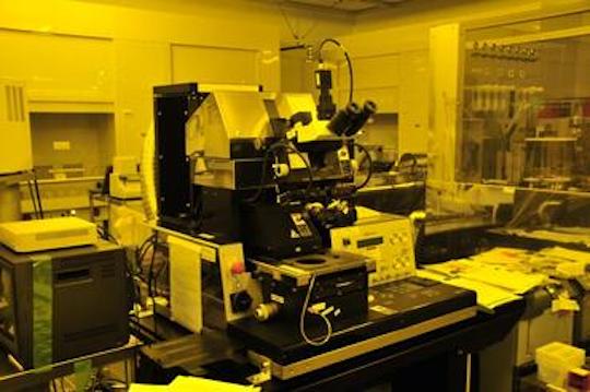
【Eniglish】Mask Aligner SUSS MA6
【別名】MA6 マスクアライナー
【型式番号】Suss MA6
【apparatus ID】122
【機器ID】F-UT-114
【機能】精密な位置合わせ(表裏1ミクロン精度)が可能で、欠片から6インチまでの露光が可能なマスクアライナーです。普段は混合で利用していますが必要であればi線フィルターをかけることができます。
【Alias】MA6 Mask aligner
【Model Number】Suss MA6
【Apparatus ID】 122
【Equipment ID】F-UT-114
【Specifications】Precise alignment (about 1um for top side alignment) is possible. Can handle many type of substrates from small chips up to 6'' wafers.
光露光(マスクレス、直接描画)
Light exposure (maskless, direct drawing)
マスクレス露光装置は、PC上で作画した任意のパターンデータを、フォトマスクを用いることなく直接基板上のフォトレジストに転写できる露光装置である。He-Cdレーザー(λ=442nm)などの光源を用い、最少描画パターン1μm程度を実現している。マスクを作る必要がないので、研究開発試作や少量カスタム生産に適している。MEMSデバイス パターンの直接描画や、露光用マスクパターン作製に使用されている。
Maskless Exposure System is an exposure system that can transfer arbitrary pattern data drawn on a PC directly onto a photoresist on a substrate without using a photomask. Using a light source such as a He-Cd laser (λ=442nm), we have achieved a minimum pattern size of about 1μm. Since there is no need to make masks, maskless lithography systems are suitable for R&D prototyping and small-volume custom production, and are used for direct imaging of MEMS device patterns and mask patterning for lithography.
レーザー直接描画装置
Laser Drawing System
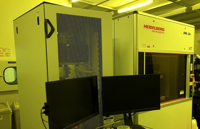
【Eniglish】Laser Drawing System
【別名】DWL66+
【型式番号】HEIDELBERG DWL66+
【apparatus ID】170
【機器ID】F-UT-146
【機能】波長406nm 小片アライメントオプション、両面アライメント機能付き。
1024階調の「グレイスケールリソグラフィー」により,フォトレジストの立体形状段差をある程度自由に作れます。また、GenISys社の変換ソフトウェア「BEAMER」を使うと、形状を得るために、近接効果の影響を計算して露光補正をしてくれます。
【Alias】DWL66+
【Model Number】HEIDELBERG DWL66+
【Apparatus ID】170
【Equipment ID】F-UT-146
【Specifications】Can handle many type of substrates from small chips up to 9''x9''. Top side and back side alignment available. Greyscale lithography with 1024 gradation.
電子線描画(EB)
Electron Beam Drawing (EB)
電子線描画は、電子銃から発せられた電子線を電子レンズや、偏向器などを通し、微細に制御されるX-Y-Zステージ上の試料に照射して目的のパターンを描画する。ビーム径はnmオーダーであり、数十nm~数nmの微細パターン描画が可能である。可変整形ビーム型では電子ビームを途中のアパーチャーで矩形にして、照射ビーム断面積を大きくして、描画速度を高めている。電子線露光装置は露光用マスク(レチクル)の作製に使われるが、研究開発用や少量生産用のデバイスの直接描画に適している。
In electron beam writing, an electron beam emitted from an electron gun is passed through an electron lens or a deflector and irradiated onto a sample on a finely controlled X-Y-Z stage to write the desired pattern. The beam diameter is on the order of nm, and it is possible to write fine patterns of tens of nm to several nm. In the variable-shape beam type, the electron beam is rectified at an aperture in the middle of the beam to increase the cross-sectional area of the irradiated beam, thus increasing the writing speed. Although electron beam lithography is used to create masks (reticles) for exposure, it is suitable for direct imaging of devices for research and development and small-lot production.
高速大面積電子線描画装置
Ultrarapid Electron Beam Direct Writing and Photo Mask Fabrication Machine
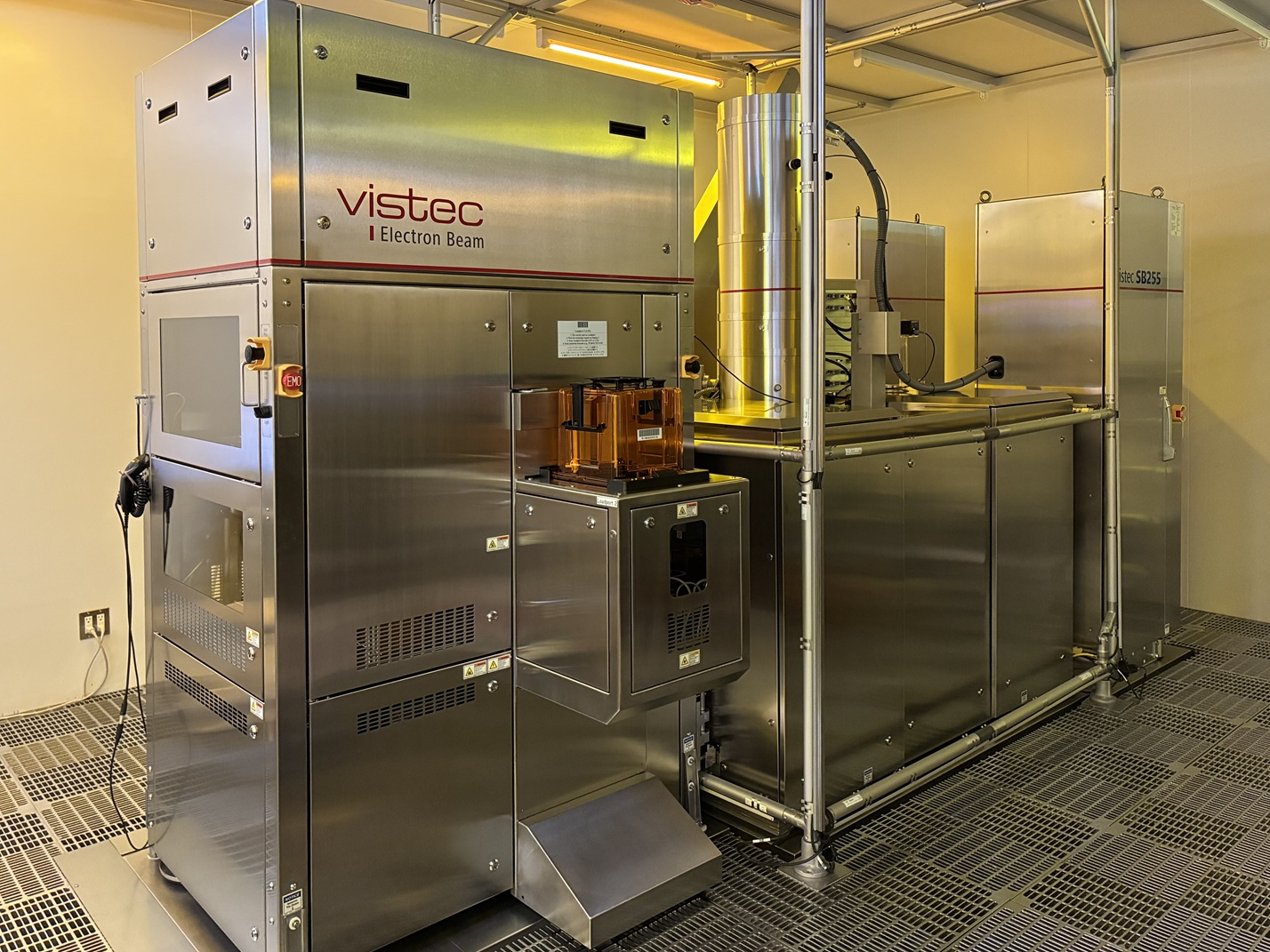
【Eniglish】Ultrarapid Electron Beam Direct Writing and Photo Mask Fabrication Machine
【別名】SB255 電子線描画装置
【型式番号】EB lithography Vistec SB255
【apparatus ID】263
【機器ID】F-UT-516
【機能】長方形矩形の大きさを任意に変更してショットすることのできる高速電子線描画装置。カケラ基板から8インチ丸基板までの任意形状に対応
【Alias】F5112 electron beam writing device
【Model Number】EB lithography Vistec SB255
【Apparatus ID】263
【Equipment ID】F-UT-516
【Specifications】It is a high-speed electron beam writing device that can change the size of rectangular rectangle to any size and shot. It can be used for any shape from a chipboard to an 8-inch round substrate.
超高速大面積電子線描画装置
Ultrarapid Electron Beam Direct Writing and Photo Mask Fabrication Machine
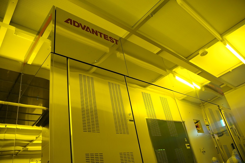
【Eniglish】Ultrarapid Electron Beam Direct Writing and Photo Mask Fabrication Machine
【別名】F7000S 電子線描画装置
【型式番号】EB lithography ADVANTEST F7000-VD02
【apparatus ID】131
【機器ID】F-UT-113
【機能】カケラから8インチ丸基板までの任意形状に対応。(厚みに制限あり。ご相談ください)可変整形ビーム(VSBモード)による、高速描画が可能。内蔵ステンシル(CPモード)による、階段近似の無い滑らかな曲線等の高速描画が可能。データはGDS-IIストリームフォーマットから変換。
【Alias】F7000S electron beam writing device
【Model Number】EB lithography ADVANTEST F7000S-VD02
【Apparatus ID】131
【Equipment ID】F-UT-113
【Specifications】Can handle many type of substrates from small chips up to 8'' wafers (there are limitation regarding the thickness, please contact us). Ultrafast EB lithography is possible thanks to variable shaped beam (VSB) mode. Thanks to built-in stencils, ultrafast exposure of smooth curves without step approximations is possible. The data are converted from GDS stream format.
レジスト塗布・現像装置
Resist coater,developer
ホトリソグラフィーにおいて露光前にウェハにレジストを塗布する方法として一般にスピンコートを行う。平坦面に均一にレジスト薄膜を形成するために、ウェーハ上にホトレジスト液を一定量滴下し、ウェーハを高速回転し、遠心力によって塗布する。なお、表面に凹凸がある場合はこの方式は適用できず、スプレー方式でレジストを塗布する。露光後、現像プロセスを経て、パターンを形成する。
In photolithography, spin coating is generally used to coat the wafer prior to exposure. To form a uniform resist film on a flat surface, a fixed amount of photoresist solution is dropped onto the wafer, and the wafer is rotated at high speed and coated by centrifugal force. If the surface is uneven, this method is not applicable, and the resist is applied by the spray method. After exposure, the pattern is formed through the development process.
マスク・ウエーハ自動現像装置群(Photomask Dev. Ash. Etcher)
Mask wafer automatic developer group(Photomask Dev. Ash. Etcher)
【Eniglish】Photomask Dev. Ash. Etcher
【別名】フォトマスク現像・アッシング・エッチング
【型式番号】EVG101
【apparatus ID】116
【機器ID】F-UT-100-1
【機能】フォトマスク(5009)作製を行うための自動処理装置ですが、EVG101は5”マスクの現像のほか、TMAHを用いたに3~8”ウエーハ現像可
【Alias】
【Model Number】EVG101
【Apparatus ID】116
【Equipment ID】F-UT-100-1
【Specifications】The EVG101 is an automatic processing machine for photomask (5009), but the EVG101 can develop 5" masks as well as 3 to 8" wafers using TMAH.
マスク・ウエーハ自動現像装置群(RIE samco FA-1)
Mask wafer automatic developer group(RIE samco FA-1)
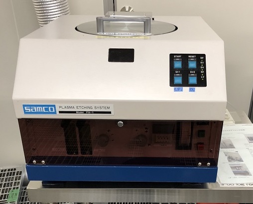
【Eniglish】RIE samco FA-1
【別名】アッシング装置 SAMCO FA-1
【型式番号】SAMCO FA-1
【apparatus ID】174
【機器ID】F-UT-100-3
【機能】半導体チップの欠陥解析を行うコンパクトな卓上型ドライエッチング装置です。パッシベーション膜を効率的かつ低ダメージで除去することが可能。試料は最大ø4 inchまで処理できます。半導体チップの欠陥解析、各種パッシベーション膜の除去、フォトレジストのアッシング、各種シリコン薄膜のエッチング、ガラス基板などの表面処理に利用可能。
【Alias】
【Model Number】SAMCO FA-1
【Apparatus ID】174
【Equipment ID】F-UT-100-3
【Specifications】Compact desktop dry etching system for semiconductor chip defect analysis. It is capable of removing passivation film efficiently and with low damage. Sample size up to ø4 inch can be processed. This system can be used for defect analysis of semiconductor chips, removal of various passivation films, ashing of photoresist, etching of various silicon thin films, and surface treatment of glass substrates.
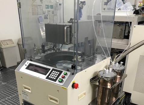
枚葉式ZEP520自動現像装置
Auto developer Actes ADE-3000S
【Eniglish】Auto developer Actes ADE-3000S
【別名】ADE-3000S 小型自動現像装置
【型式番号】アクテス京三 ADE-3000S
【apparatus ID】165
【機器ID】F-UT-152
【機能】 CR1奥、ドラフトチャンバの右側にあります。ZEP520A (-7)専用自動現像装置。3inchから8inchのSiliconまたガラスのWaferで利用可能、Chipは不可。
【Alias】
【Model Number】Actes Kyosan ADE-3000S
【Apparatus ID】165
【Equipment ID】F-UT-152
【Specifications】The ADE300S is located at the back of CR1, to the right of the draft chamber, and is a dedicated automatic developer for ZEP520A (-7). 3-inch to 8-inch silicon and glass wafers are available, but chips are not.
スプレーコーター
Spray Coater
【Eniglish】Spray Coater
【別名】Spray Coater ACTIVE ACT-300AIIS
【型式番号】ACTIVE ACT-300AⅡS
【apparatus ID】180
【機器ID】F-UT-156
【機能】Φ5~Φ150 (Max.Φ6インチ、□110mm)の基板対応
【Alias】Spray Coater ACTIVE ACT-300AIIS
【Model Number】ACTIVE ACT-300AⅡS
【Apparatus ID】180
【Equipment ID】F-UT-156
【Specifications】Φ5~Φ150 (Max.Φ6inch、□110mm)
DC111 スプレーコーター
DC111 Spray Coater
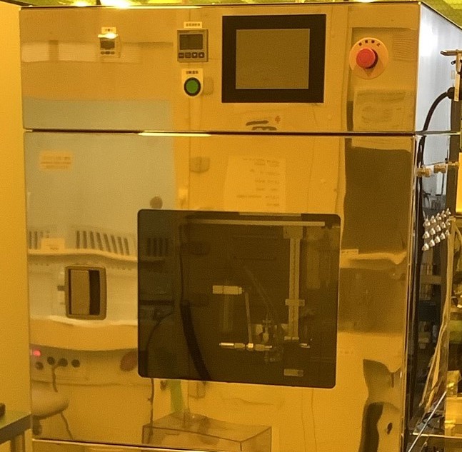
【Eniglish】DC111 Spray Coater
【別名】DC111 スプレーコータ
【型式番号】DC111
【apparatus ID】
【機器ID】
【機能】フォトレジスト等の塗布液をスプレーによりコーティングする装置。サンプル凸凹面へ均一に膜を形成可能で、従来のスピンナーでは実現が難しいキャビティ、トレンチ構造への埋め込み塗布も可能です。
試料台サイズ:220x220㎜(ヒータ内蔵 ~100℃)、ノズル移動速度:10-300㎜/s、ノズル移動範囲:300x300mm
【Alias】DC111 Spray Coater
【Model Number】DC111
【Apparatus ID】
【Equipment ID】
【Specifications】A system for coating photoresist and other coating liquids by spraying. The system is capable of forming a uniform film on the uneven surface of a sample, and can also perform embedded coating in cavity and trench structures, which is difficult to achieve with conventional spinners.
Sample table size: 220 x 220 mm (with built-in heater up to 100°C), nozzle movement speed: 10-300 mm/s, nozzle movement range: 300 x 300 mm