受賞と成果に関するニュース
News related to awards and achievements
令和3年度「秀でた利用成果」最優秀賞受賞しました。3年連続受賞・内2年連続最優秀の快挙!
We got the best award of "Excellent Use Results." This is the brilliant achievement of 2 years series about the best awards, 3 years the awards!
「プラズモニック構造を利用したシリコンMEMSモノリシック赤外SPR分光センサ」
ユーザー氏名 :
菅哲朗、大下雅昭、安永竣 (電気通信大学)
実施機関担当者 :
澤村智紀、Eric Lebrasseur、藤原誠、岡本有貴(現在、産総研)、水島彩子、宇佐美尚人(現在、JAXA/ISAS)、肥後昭男、太田悦子、三田吉郎(東京大学)
文部科学省ナノテクノロジープラットフォーム事業では毎年、3,000件を超える利用報告書の中から厳正な審査の上、「秀でた利用成果」を顕彰しています。2021年12月20日、令和3年度「秀でた利用成果」が発表され、東京大学微細加工拠点の利用成果が「最優秀賞」を受賞しました。令和元年度(受賞4件)、2年度(大賞1件)、3年度(大賞1件)の連続受賞です。確率で計算すると「27,000,000,000分の4」(270億分の4)という、価値ある受賞です。
電気通信大学の菅哲朗教授のグループは、東京大学超微細リソグラフィー・ナノ計測拠点の利用により、プラズモン共鳴の原理を用いて安価なシリコン材料で赤外線検出を可能とし、さらにMEMS角度走査アクチュエータにセンサを搭載することにより波長選択型の超小型・軽量・高性能で安価なシリコン製赤外センサを世界で初めて実現しました。当拠点からは、シリコン製MEMS赤外線センサの試作において、拠点が長年培ってきた高精度な微細加工技術を提供し、経験豊かな技術スタッフによる技術支援により設計通りの高性能なセンサを実現することに貢献しました。
授賞式ならびに講演会が、東京ビッグサイトで2022年1月26-28日に開催されるnanotech2022において1月26日に執り行われます。併せて3日間ポスター発表が行われます。是非お越しください。
"Silicone MEMS monolithic infrared SPR spectroscopic sensor employing plasmonic structure"
User Name :
Tetsuro Kan, Masaaki Oshita, Shun Yasunaga (The University of Electro-Communications)
Implementing Agency Representative :
Tomoki Sawamura, Eric Lebrasseur, Makoto Sawamura, Yuki Okamoto (Now AIST), Ayako Mizushima, Naoto Usami (Now JAXA/ISAS), Akio Higo, Etsuko Ota, Yoshio Mita (The University of Tokyo)
Every year, nanotechnology platform of the Ministry of Education, Culture, Sports, Science and Technology gives prize to "Excellent Use Results" through the strict review of over 3000 application reports. At 2021/12/20 the "Excellent Use Result" in 2021 was presented and the utilization achievement from the nanotechnology platform in The University of Tokyo got "The Best Award." This accomplishment follows 2019 (4 rewards) and 2020 (1 first prize.) This is much valuable winning, which is “4/27,000,000,000” as probability.
The research group of Assoc. Prof. Tetsuro Kan in The University of Electro-Communications realized wave-selective ultra-small, light, highly efficient and inexpensive Si infrared sensor first in the world, which was composed of MEMS angular scanning actuator with the Si low-cost sensor enabling the detection of infrared rays from the theory of Plasmon Resonance, partly manufactured in the nanotechnology platform in The University of Tokyo. In our facility, experienced engineering staff helped the group make the Si MEMS infrared sensor with high performance as designed, providing precisely nanotechnological processing skill cultivated for years.
The award ceremony and lecture will be held at 2022/1/26 in Tokyo Big Site, during nanotech2022 from 2022/1/26 to 28. The poster presentation will also take place for 3 days. Please come and join us.
令和2年度「秀でた利用成果」最優秀賞受賞!
We were awarded the Grand Prize for Outstanding Achievement in 2020!
「熱アシストハードディスク用微小光熱源 ナノヒーター®素子」
ユーザー氏名 :
杉浦 聡a, 井上 友里恵f, 橋本 和信f, 望月 学a,f, 八井 崇b,f,
赤羽 浩一c, 松本 敦c, 山本 直克c, 片山 龍一d, James A. Baine
(a(株)イノバステラ, b豊橋技術科学大学, c情報通信研究機構, d福岡工業大学, eCarnegie Mellon Univ.,fナノフォトニクス工学推進機構)
実施機関担当者 :
澤村 智紀, 水島 彩子, 太田 悦子, Eric Lebrasseur, 藤原 誠 (東京大学)
株式会社イノバステラを筆頭とする共同研究グループは、東京大学超微細リソグラフィ・ナノ計測拠点の利用により、ハードディスクドライブ(HDD)の記録密度を10倍にすることができる「熱アシスト磁気記録方式」を実現するナノヒーター®を開発しました。当拠点は、ナノヒーター®の試作において、拠点が長年培ってきた高精度な微細加工技術を提供し、経験豊かな技術スタッフによる技術支援により設計通りの高性能なナノヒーターデバイスを実現することに貢献しました。この成果が、文部科学省ナノテクノロジープラットフォーム令和2年度「秀でた利用成果」最優秀賞に選定されました。
"Micro-optical heat source for heat-assisted hard disks, nano-heater® device"
User Name :
Satoshi Sugiura a, Yurie Inoue f, Kazunobu Hashimoto f, Manabu Mochizuki a,f, Takashi Yai b,f,
Koichi Akahanec, Atsushi Matsumotoc, Naokatsu Yamamotoc, Ryuichi Katayamad, James A. Baine
(aInovastera Corporation, boyohashi University of Technology, cNational Institute of Information and Communications Technology, dFukuoka Institute of Technology, eCarnegie Mellon Univ, fOrganization for the Promotion of Nanophotonics Engineering)
Implementing Agency Representative :
Tomonori Sawamura, Ayako Mizushima, Etsuko Ohta, Eric Lebrasseur, Makoto Fujiwara (University of Tokyo)
In today's digital society, electronic information is increasing rapidly, and the development of technology to significantly increase the storage density of hard disks while maintaining current power consumption is becoming increasingly important. The next generation of hard disk recording methods that can significantly increase the storage density is the heat-assisted magnetic recording method. With this method, magnetic recording must be performed by locally heating an area of about 10 nm in diameter. We have developed a micro-optical heat source device fabricated from a GaAs substrate using the University of Tokyo's microfabrication platform. As a result, a heat source with a small number of parts and a heating area of about 10 nm has been realized for the first time.
格子状に並んだナノサイズの穴を持つ薄い膜が、らせんの光の波長を変える
An article entitled "Circularly polarized vacuum ultraviolet coherent light generation using a square lattice photonic crystal nanomembrane" was published in a top journal of the field. The TakedaCR team is happy to share this news as one of the examples of fruitful collaboration of specialists of divers resaearch domains.
理学系研究科小西邦昭先生(五神・湯本研)と三田吉郎准教授の共著トップジャーナル掲載論文に関するプレスリリースが刊行されました。
「格子状に並んだナノサイズの穴を持つ薄い膜が、らせんの光の波長を変える」
~極短波長のそろった円偏光を簡単に作り出すことに成功~
五神・湯本研究室は、武田先端知スーパークリーンルーム運営の中核研究室の一つで、小西邦昭先生(フォトンサイエンス研究機構助教)は、ヘビーユーザです。当時、三田吉郎准教授のグループは企業との共同研究で、バイオデバイス応用を目指した「微細孔加工を施したメンブレン構造MEMSデバイス」の研究を行なっていました。ある日小西先生より相談を受け、開発していた加工技術が真空紫外応用に転用出来ると案内したことが本研究の短期間での実現の鍵の一つとなりました。初期成果を得た後も、継続的に半導体微細加工の専門家としての立場で最適材料や構造作製、論文投稿に至る研究遂行に協力し、トップジャーナルでの共著論文発表につながりました。研究協力は継続しており、微細構造付きメンブレン作製手法の学術論文は三田研が責任著者となって共著論文発表を行なっています。このように、異分野の専門家が得意分野を持ち寄って新規デバイス・システムを実現するオープンプラットフォームとして「文部科学省ナノテクノジープラットフォーム東京大学微細加工拠点」は160を超える研究室より700名近くの利用者が日々切磋琢磨しています。
Gokami-Yumoto Laboratory is one of the core laboratories of Takeda Super Clean Room. Prof. Kuniaki Konishi (Assistant Professor at Photon Science Institute) is a heavy user. Since several years, Associate Professor Yoshio Mita's group have been conducting research on "MEMS devices with micropore-processed membrane structure" for biodevice applications as a joint research with industry. One day, Dr. Mita talked in Takeda (in memory, it was in cleanroom warering room) with Dr Konishi on his new idea. Dr. Mita told to Dr. Konishi that the required process technology was just under development, and it could be applied to his vacuum ultraviolet (VUV) application. This was one of starting points towards realization of this research in a short period of time. After obtaining the initial results, we (TakedaCR support team) continued to cooperate with him as an expert in semiconductor microfabrication and helped him to carry out his research, including the fabrication of optimal materials and structures and submission of papers, which led to the publication of joint papers in a top journal. The research collaboration continues, and we have co-authored a paper on the fabrication of microstructured membranes. Likewise, nearly 700 users from more than 160 laboratories are engaged in friendly competition with each other every day in the "MEXT Nanotechnology Platform - Nanofabrication Center at the University of Tokyo" as an open platform for realizing new devices and systems with experts in different fields bringing their expertise.
令和元年度ナノテク「秀でた成果」優秀賞受賞
We were awarded the Grand Prize for Outstanding Achievement in 2019!
文部科学省ナノテクノロジープラットフォーム秀でた利用成果 解説記事に寄稿しました!
<2020年秀でた利用成果-3>21世紀の「黄金の国ジパング」を目指して
~ナノテクノロジープラットフォーム東京大学微細加工拠点による光触媒・ 超親水性機能融合反射防止多層膜材料の開発~
超親水機能・光触媒機能を兼ね備えた反射防止誘電体多層膜
ユーザー:多田 一成、水町 靖 (コニカミノルタ株会社)
実施機関担当:澤村智紀、藤原誠、水島彩子、Eric Lebrasseur、太田悦子 (東京大学)
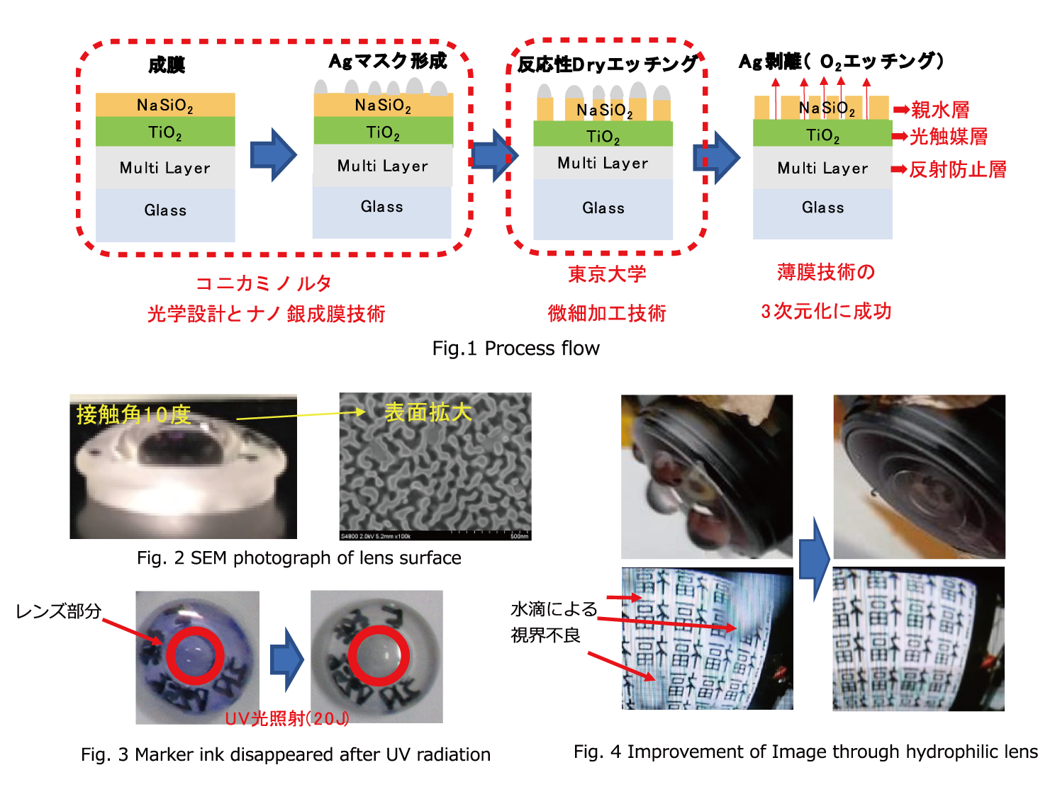
近年増加している車載やセンサーカメラなどでの水滴の映り込みを防ぎ、常にクリアな視界を提供する為、超親水機能と光触媒によるクリーニング機能を兼ね備えた反射防止膜を開発した。再表面にある超親水性NaSiO2層と、その下に配置された光触媒機能を持つTiO2層を、エッチングによる微細加工を用いて貫通穴を掘ることで縦に3次元的にコネクトした。このナノサイズの穴を通り光触媒が表面層に発現する為、2つの異なる材料の膜の望ましい特徴を、表面に同時に発現できる3次元光学薄膜を得ることができた。
製造プロセス:社内にて光学レンズ上に下地となる反射防止多層膜を成膜した後、アナターゼ型TiO2とNaSiO2の連続成膜を行った。次に自己組織的ナノネットワーク構造を持ったAgマスクを蒸着した。最後に微細加工プラットフォームの設備CE-300Iを用いて、CHF3反応性エッチングを行いSiO2膜を89nm程掘り込むことで下層のTiO2層を部分的に剥き出しにすることに成功した(Fig.1)。
結果:作製後のレンズ表面SEM画像をFig. 2に示す。幅50-200nmの微細な溝がネットワーク上に形成されていることが確認できる。光触媒は、UV光照射によりメチレンブルーのインクが消失することで確認した(Fig. 3)。また親水性は、水滴の接触角が10°であることで確認した。最後にこのレンズを用いた画質改善(水滴による視界不良の解決)をFig.4に示す。以上から、光触媒効果を持ちながら超親水性を示す反射防止コートを実現することができた。
I contributed to the commentary article about the excellent use results of the nanotechnology platform of the Ministry of Education, Culture, Sports, Science and Technology!
<Outstanding use results-3 in 2020> Aiming for the “Golden Country Zipangu” in the 21st century
-Nanotechnology Platform Photocatalyst by the University of Tokyo
Recipient of the first year of Reiwa (2020) "outstanding result" award for excellence.
Antireflection coating with both super-hydrophilicity and photocatalysis effect
Users: Kazunari Tada, Yasushi Mizumachi (KONICA MINOLTA, INC.)
Supporting staff: Tomoki Sawamura, Makoto Fujiwara, Ayako Mizushima, Eric Lebrasseur, Etsuko Ohta (The Univ. of Tokyo)
Anti-reflection coating to simultaneously realize super-hydrophilicity and photocatalysis is successfully developed in order to provide a clear view for recently increasing sensing camera lenses. Super-hydrophilic NaSiO2 layer on the surface and underlying photocatalytic TiO2 layer are connected via nano-structured tunnels fabricated by dry etching technique to obtain two different favorable functions combined together at the surface of a lens.
Fabrication process: In our company, a multilayer antireflection film is deposited on an optical lens. Then anatase-type TiO2 and NaSiO2 are deposited successively. Next, Ag is evaporated and form a self-organized nano-network structure which is used as an etching mask. Finally, 89nm SiO2 layer is etched with CHF3 gas, using the nanofabrication platform ICP-RIE CE-300I machine, leaving partly exposed the TiO2 layer (Fig.1).
Result: The Fig.2 shows a SEM image of the lens surface after fabrication. We can see a network of 50 to 200nm width lines. We can observe that under UV irradiation, the methylene blue ink disappears thanks to the photocatalyst action (Fig.3). We also checked that thanks to the hydrophilic surface, the contact angle of the water droplets is 10°C. Finally, improvement of the image quality is shown on Fig.4. In conclusion, an antireflection and superhydrophilic coating with photocatalyst effect has been demonstrated.