形状・形態観察、分析
Shape and form observation and analysis
材料やデバイス研究開発の過程では、形状・形態観察、物理分析が必要となる。形状・形態観察に関しては光・電子の各種顕微鏡類、プローブ顕微鏡、膜厚測定などの各種装置が揃っている。分析についても、分光分析で各種波長の電磁波、イオン、プラズマを活用するシステムが存在する。これらの機器・装置の多くは微細構造解析プラットフォームの機器・装置と共通である。
Shape and form observation and physical analysis are necessary for research and development of materials and devices. For shape and form observation, various types of equipment are available, such as light and electron microscopes, probe microscopes, and film thickness measurement. For analysis, there are systems that utilize electromagnetic waves, ions, and plasma of various wavelengths for spectroscopic analysis. Many of these instruments and devices are the same as those used in the Microstructure Analysis Platform.
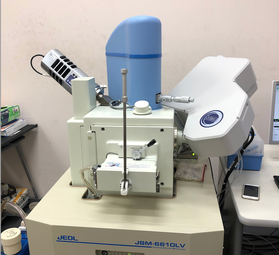
走査電子顕微鏡(SEM)
SEM(Scanning Electron Microscope)
SEM(Scanning Electron Microscope)は、電子線を加速・集束して得た電子プローブを試料表面に照射・走査し、対象物から放出される二次電子、反射電子、透過電子、X線、蛍光、内部起電力等を検出、その映像を拡大表示して対象を観察する顕微鏡。通常は二次電子像が利用される。像の分解能は電子線の直径で決まり、直径は熱陰極電子銃で2~10 nm、電界放射電子銃で0.5~2 nm。
SEM (Scanning Electron Microscope) is a microscope that irradiates and scans a sample surface with an electron probe obtained by accelerating and focusing an electron beam, detects secondary electrons, reflected electrons, transmitted electrons, X-rays, fluorescence, internal electromotive force, etc. emitted from the object, and magnifies the image to observe the object. Usually, secondary electron images are used. The resolution of the image is determined by the diameter of the electron beam, which is 2 to 10 nm for a hot-cathode electron gun and 0.5 to 2 nm for a field emission electron gun.
SEM
【英語】SEM
【別名】
【型式番号】日本電子JSM-6610LV EDS付
【apparatus ID】
【機器ID】F-UT-
【機能】
【Alias】
【Model Number】Japan Electronics Corporation JSM-6610LV with EDS
【Apparatus ID】
【Equipment ID】F-UT-
【Specifications】
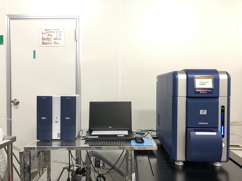
SEM
【英語】SEM
【別名】
【型式番号】日立卓上顕微鏡 TM-3030Plus
【apparatus ID】119
【機器ID】F-UT-145
【機能】
【Alias】
【Model Number】HITACHI TM-3030Plus
【Apparatus ID】119
【Equipment ID】F-UT-145
【Specifications】
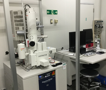
高精細電子顕微鏡
Ultra-high Resolution Scanning Electron Microscope
【英語】Ultra-high Resolution Scanning Electron Microscope
【別名】FE-SEM Hitachi Regulus8230
【型式番号】HITACHI Regulus 8230
【apparatus ID】175
【機器ID】F-UT-151
【機能】
【Alias】FE-SEM Hitachi Regulus8230
【Model Number】HITACHI Regulus 8230
【Apparatus ID】175
【Equipment ID】F-UT-151
【Specifications】
走査プローブ顕微鏡(SPM)
SPM(Scanning Probe Microscope)
SPM(Scanning Probe Microscope)は、先端を尖らせた探針(プローブ)を物質の表面に近づけてプローブ直下の表面に刺激を与えた時の応答を測定し、プローブを動かした時の応答から、原子配列、電子構造、凹凸などの表面状態をナノメートルオーダーの空間分解能で2次元的に拡大観察することのできる顕微鏡です。
SPM (Scanning Probe Microscope) is a microscope that enables two-dimensional magnified observation of surface conditions such as atomic arrangement, electronic structure, and unevenness with nanometer-order spatial resolution. A probe with a pointed tip is brought close to the surface of a material, and the response to stimulation of the surface directly under the probe is measured. Observation data is acquired from the response when the probe is moved.
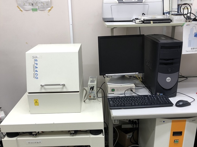
小型原子間力顕微鏡
Atomin Force Microscope (AFM)
【英語】Atomin Force Microscope (AFM)
【別名】
【型式番号】SPA400+SPI4000
【apparatus ID】
【機器ID】F-UT-165
【機能】プローブステーション(工学部2号館電子顕微鏡室)
【Alias】
【Model Number】SPA400+SPI4000
【Apparatus ID】175
【Equipment ID】F-UT-165
【Specifications】Probe Station (Electron Microscope Room, Engineering Bldg. 2)
分光(光、電子線、イオン線、プラズマ、磁気、X線)
Spectroscopy (light, electron beam, ion beam, plasma, magnetism, X-ray)
分光法は分光器によって発光および吸収スペクトルを調べる物理分析法である。γ線、X線、紫外線、可視光線、赤外線、マイクロ波の各種波長領域について発光および吸収スペクトルから物質の同定、定性、定量を行う手法がある。
Spectroscopy is a physical analysis method that examines emission and absorption spectra using a spectroscope, and includes methods for identifying, qualifying, and quantifying substances based on emission and absorption spectra in various wavelength regions, such as gamma rays, X-rays, ultraviolet rays, visible light, infrared rays, and microwaves.
オージェ分光分析装置
Auger Electron Spectroscopy
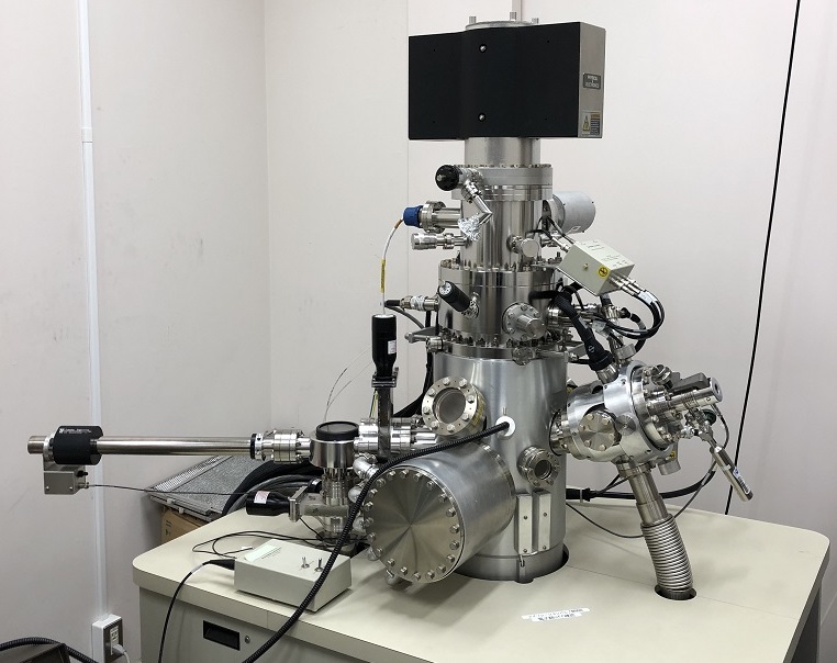
【英語】Auger Electron Spectroscopy
【別名】
【型式番号】ULVAC PHI680
【apparatus ID】
【機器ID】F-UT-150
【機能】元素分析装置。
対象の極表面から出て来るオージェ電子のエネルギー分光計測によって元素を調べることが出来る。
アルゴンミリングと併用でき、深さ方向のプロファイルを測定することができる。
【Alias】
【Model Number】ULVAC PHI680
【Apparatus ID】
【Equipment ID】F-UT-150
【Specifications】Elemental analyzer.It can investigate elements by measuring the energy spectra of Auger electrons emitted from the extreme surface of the target.Can be used in conjunction with argon milling to measure depth profiles.
光学顕微鏡(一般、共焦点、レーザ)
Optical Microscopes (General, Confocal, Laser)
光学顕微鏡類としては、レーザー顕微鏡(生物用共焦点レーザ走査型顕微鏡、3D測定レーザー顕微鏡など)、デジタル顕微鏡(測微機能および3次元表示機能付き)、蛍光イメージングシステム(蛍光顕微鏡とサポートシステム)などがある。
Optical microscopes include laser microscopes (e.g., biological confocal laser scanning microscopes, 3D measurement laser microscopes), digital microscopes (with microscopy and 3D display functions), and fluorescence imaging systems (fluorescence microscopes and support systems).
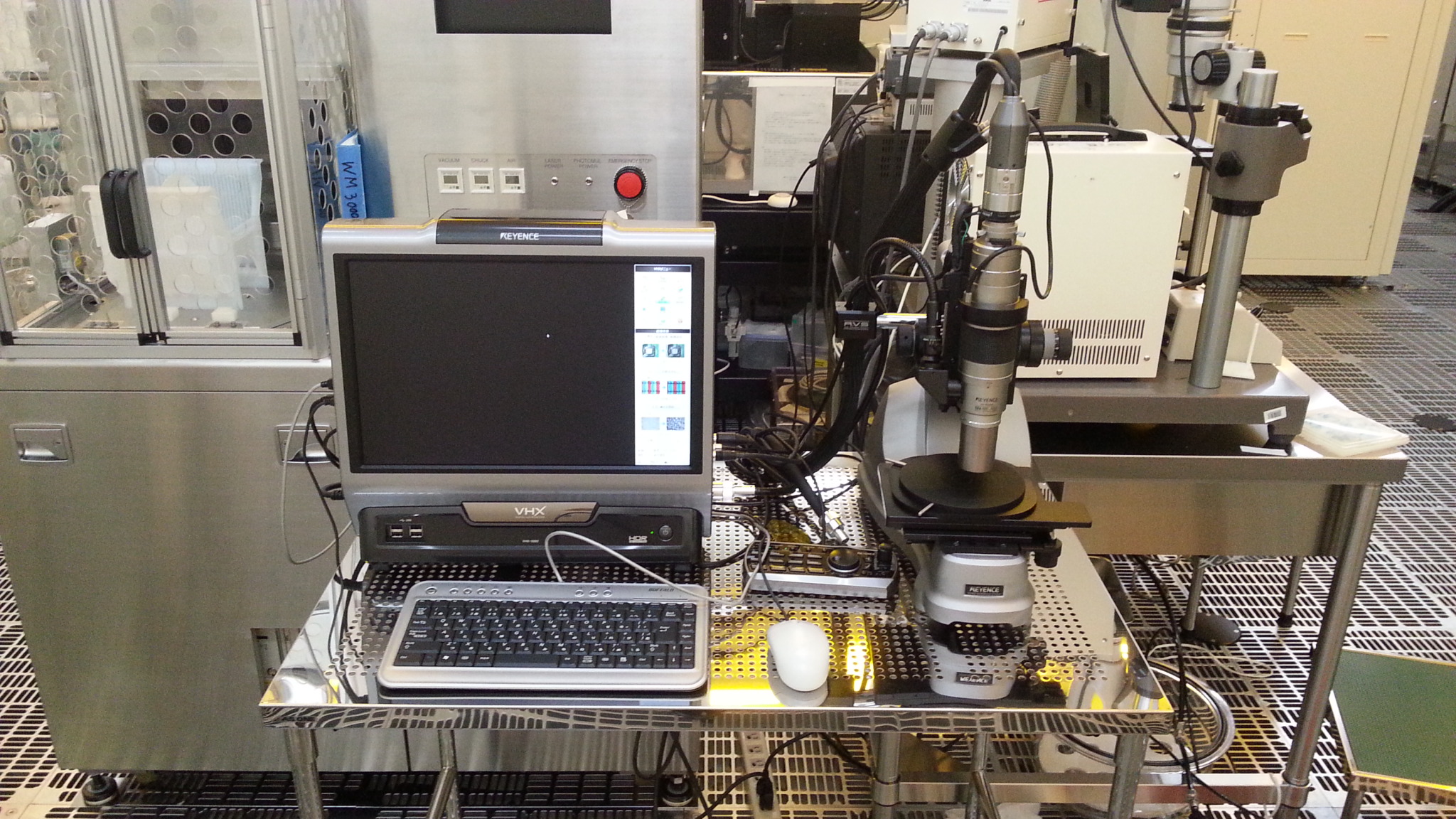
形状・膜厚・電気特性評価装置群
Series of analysis equipments, visual, thickness, and electrical/mechanical characteristic.
【英語】
【別名】Keyence顕微鏡
【型式番号】VHX-6000
【apparatus ID】
【機器ID】F-UT-105-1
【機能】顕微鏡観察を行う装置です。
【Alias】Keyence Microscope
【Model Number】VHX-6000
【Apparatus ID】
【Equipment ID】F-UT-105-1
【Specifications】This is a device for microscopic observation.
膜厚・段差・粗さ測定
Film thickness, step and roughness measurement
膜厚・段差の測定では、垂直解像度1nmの触針式表面形状測定装置、膜の表面と裏面で反射した光の干渉を利用する光干渉方式(60μmまでのレジスト膜厚測定可、最大4層膜まで同時測定可)、Åレベルの薄い膜に対して良い感度を持つ分光エリプソメトリー(薄膜の屈折率nと消衰係数k(光学定数)や、膜厚、表面粗さ・界面の粗さなどを測定できる)などがある。これらとは異なり、MEMSデバイスの動的特性(面外、面内)および表面形状を3次元で測定するマイクロシステムアナライザーがある。
For the measurement of film thickness and step, there are several methods: a tactile surface profiler with a vertical resolution of 1 nm, an optical interference method that uses the interference of light reflected from the surface and back of the film (capable of measuring resist film thicknesses of up to 60 μm and simultaneous measurement of up to four layers of film), and spectroscopic ellipsometry (capable of measuring the refractive index n and extinction coefficient k (optical constants) of thin films, as well as film thickness, surface roughness, and interface roughness). ), and spectroscopic ellipsometry (capable of measuring the refractive index n and extinction coefficient k (optical constant) of thin films, film thickness, and surface and interface roughness). Unlike these, there are micro system analyzers that measure the dynamic properties (out-of-plane and in-plane) and surface topography of MEMS devices in three dimensions.
形状・膜厚・電気特性評価装置群
Stylus profiler BRUKER DektakXT
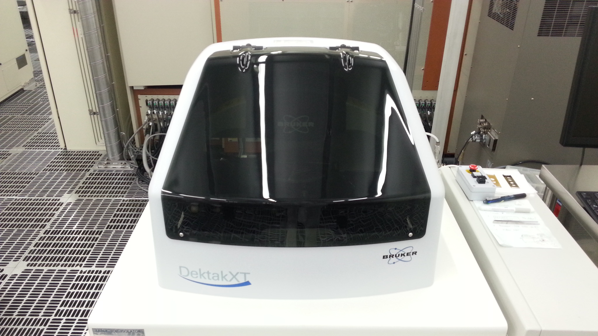
【英語】Stylus profiler BRUKER DektakXT
【別名】触針段差計
【型式番号】DektakXT-S
【apparatus ID】103
【rec ID】5
【old site No】
【機器ID】F-UT-105-2
【機能】
【Alias】
【Model Number】
【Apparatus ID】
【Equipment ID】F-UT-105-2
【Specifications】
形状・膜厚・電気特性評価装置群
TohoSpec
【英語】TohoSpec
【別名】TohoSpec
【型式番号】
【apparatus ID】197
【機器ID】
【機能】SiO2やレジスト、SiN膜の膜厚を簡易的に測定します。
【Alias】TohoSpec
【Model Number】
【Apparatus ID】197
【Equipment ID】
【Specifications】Easy SiO2, resist, SiN films measurement.
形状・膜厚・電気特性評価装置群 8インチプローバ
8-inch Probe Station
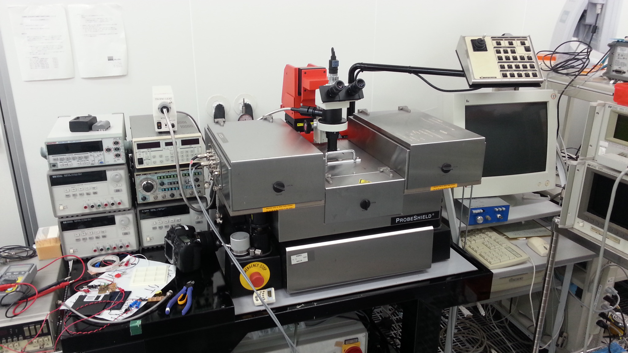
【英語】8-inch Probe Station
【別名】8インチプローバ PM8
【型式番号】
【apparatus ID】153
【機器ID】F-UT-105-4
【機能】Suss8”プローバ,針を当てて電気的特性を測定する装置です。8インチ対応。
【Alias】
【Model Number】Probe station Karl Suss PM8
【Apparatus ID】153
【Equipment ID】F-UT-105-4
【Specifications】Electrical characteristics measurement by using needle probes. Maximum sample size: 8''.
形状・膜厚・電気特性評価装置群
Ellipsometer
【英語】Ellipsometer
【別名】分光エリプソメータ―M-550
【型式番号】JASCO M-550
【apparatus ID】164
【機器ID】F-UT-105-5
【機能】
【Alias】
【Model Number】JASCO M-550
【Apparatus ID】164
【Equipment ID】F-UT-105-5
【Specifications】
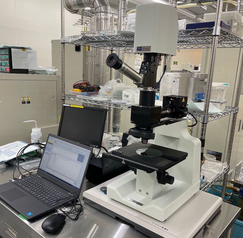
形状・膜厚・電気特性評価装置群
Laser microscope
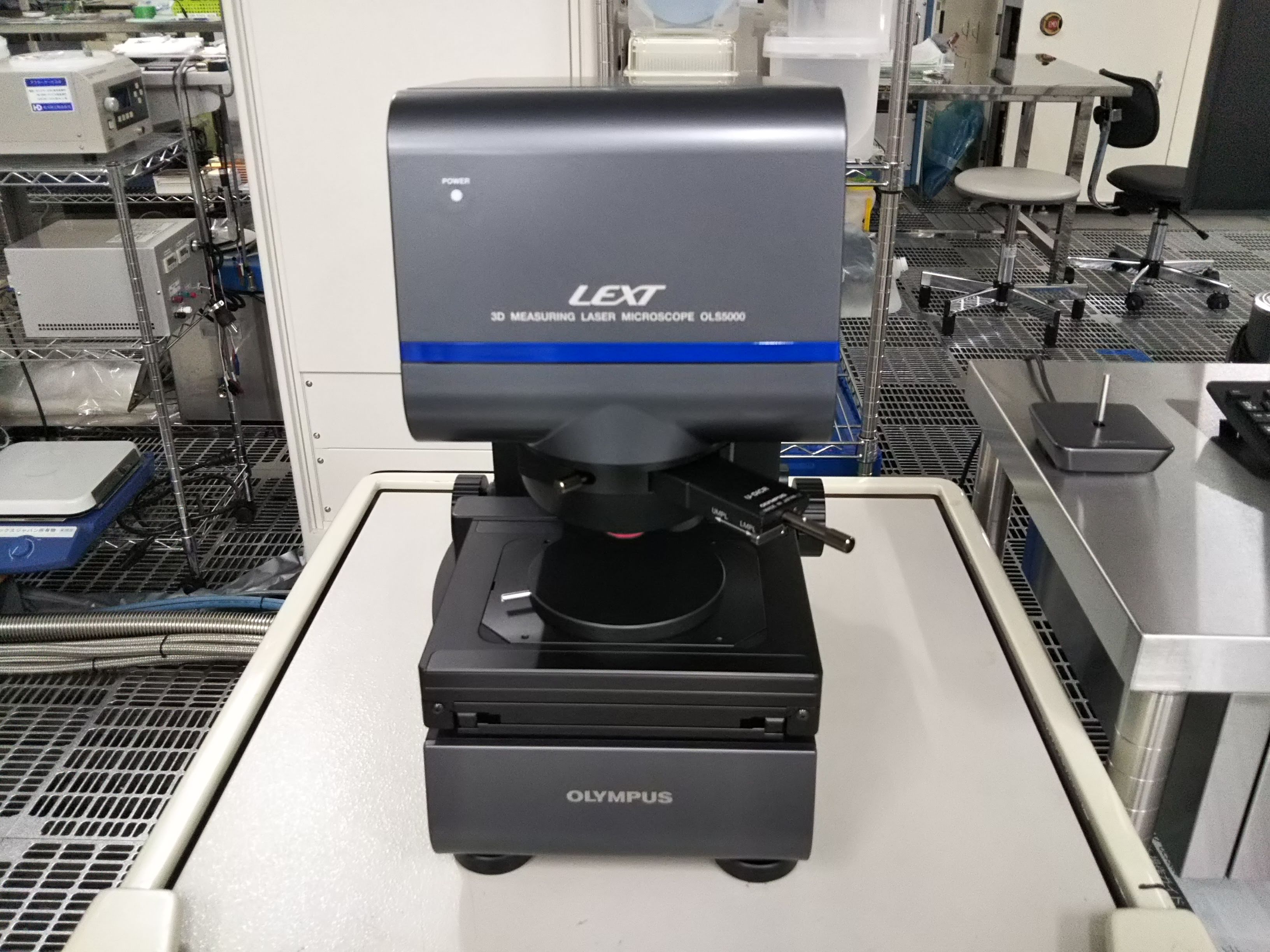
【英語】Laser microscope OLYMPUS LEXT OLS5000
【別名】レーザー顕微鏡 LEXT OLS5000
【型式番号】OLYMPUS LEXT OLS5000
【apparatus ID】169
【機器ID】F-UT-105-6
【機能】
【Alias】
【Model Number】OLYMPUS LEXT OLS5000
【Apparatus ID】169
【Equipment ID】F-UT-105-6
【Specifications】