成膜・膜堆積
Film Deposition and Film Deposition
半導体デバイス等の機能を発現するために半導体、絶縁体、金属などの薄層をチップ上に重ねて形成する。また保護膜のニーズもある。膜形成材料、膜の厚さ、品質・精度などの要求条件に対応できる各種成膜・堆積技術がある。成膜・堆積技術としては、気相法の他に、メッキなどのように液相法もある。なお、堆積とパターン形成を同時に行うもの、例えば印刷技術などはリソグラフィー・露光・描画装置の大分類に入っている。
Deposition and film deposition are the formation of thin layers of semiconductors, insulators, metals, etc., on a chip in order to develop the functions of semiconductor devices, etc. It also has a need as a protective film. There are a variety of deposition and deposition technologies that can meet the requirements for film-forming materials, film thickness, quality and precision. In addition to gas-phase deposition, there are also liquid-phase deposition methods, such as plating. In addition, those that perform deposition and patterning at the same time, such as printing technology, are included in the large category of lithography, exposure, and drawing equipment.
蒸着(抵抗加熱、電子線)
真空蒸着装置は真空にした容器の中で、蒸着材料を加熱などにより気化もしくは昇華して、離れた位置に置かれた基板の表面に付着させ、薄膜を形成する装置である。加熱手段には抵抗加熱、電子ビーム照射、高周波誘導、レーザー照射などの方法がある。真空蒸着法の長所は、膜の厚さの微妙なコントロールができることである。可能な蒸着材料はAl、Ag、Au、Ti、Ni、Cu、Cr、Sn、Inなどの金属およびAl2O3、SiO2などの酸化物である。
Vacuum evaporation (resistance heating, electron beam)
In a vacuum evaporation system, evaporation materials are vaporized or sublimated in a vacuum container by heating or other means to adhere to the surface of a substrate placed at a distance to form a thin film. Heating methods include resistance heating, electron beam irradiation, high-frequency induction, and laser irradiation. The advantage of the vacuum deposition method is that the thickness of the film can be controlled delicately. Possible deposition materials include metals such as Al, Ag, Au, Ti, Ni, Cu, Cr, Sn, and In, and oxides such as Al2O3 and SiO2.
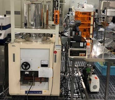
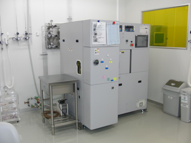
4インチ高真空EB蒸着装置
Ultra high vacuum evaporator
.jpg)
【English】Ultra high vacuum evaporator NSP2
【別名】超高真空EB蒸着装置(NSP2)
【型式番号】NSPⅡ
【apparatus ID】123
【機器ID】F-UT-102
【機能】東大拠点で独自設計・自作した蒸着装置で、いわゆる抵抗加熱蒸着と電子線(EB)加熱蒸着との両方が可能です。主な材料はAu, Cr, Alです。
【Alias】Ultra high vacuum evaporator NSP2
【Model Number】NSPⅡ
【Apparatus ID】123
【Equipment ID】F-UT-102
【Specifications】Home made evaporator. both thermal and EB evaporation are available. Main materials are Au, Cr, Al.
超高真空蒸着装置(ベルジャー)
Ultra high vacuum evaporator (Bell-jar)
【English】Ultra high vacuum evaporator (Bell-jar)
【別名】
【型式番号】
【apparatus ID】140
【機器ID】F-UT-134
【機能】抵抗加熱のみ。φ4inchまで可能
【Alias】
【Model Number】
【Apparatus ID】140
【Equipment ID】F-UT-134
【Specifications】Thermal evaporation. Can handle up to 4'' wafers.
スパッタリング
Sputtering
ターゲット(物質)にArなどの不活性な物質を高速で衝突させ、ターゲットを構成する原子や分子を叩き出し、この叩き出された原子や分子を基板上に付着させ薄膜を形成する技術をスパッタリングという。基板への付着力の強い膜の作製、合金系や化合物のターゲットの組成比をほぼ保ったまま膜作製が可能、融点の高い物質でも堆積が可能、スパッタするガスに反応性のガスを混合することによって、酸化物、窒化物の薄膜の作成も可能などの特徴がある。
Sputtering is a technique for forming thin films by bombarding a target (material) with an inert substance such as Ar at high speed to knock out the atoms and molecules that make up the target, and then attaching the knocked out atoms and molecules to the substrate. It is possible to fabricate films with strong adhesion to the substrate, and to fabricate films while maintaining almost the same composition ratio of the alloy or compound target. It is also possible to deposit even materials with high melting points. Furthermore, by mixing reactive gases with the gas to be sputtered, it is possible to create oxide and nitride thin films, among other features.
8インチ汎用スパッタ装置
General purpose Sputtering machine, ULVAC SIH-450
【English】General purpose Sputtering machine, ULVAC SIH-450
【別名】
【型式番号】ULVAC SIH-450装置
【apparatus ID】138
【機器ID】F-UT-115
【機能】4インチウエーハ8枚、8インチウエーハ2枚導入可能。6インチターゲット2枚、4インチターゲット1枚が可能。RFとDCスパッタリングが可能。Al,SiO2,TiN,Taターゲットがあります。その他のターゲット導入も相談に乗ります(在庫がない場合注文から導入まで数ヶ月かかることもありますので相談はお早めに。)
【Alias】
【Model Number】ULVAC SIH-450
【Apparatus ID】138
【Equipment ID】F-UT-115
【Specifications】Up to height 4'' wafers or two 8'' wafers can be loaded at the same time. There are two 6'' targets and one 4'' target. Both RF and DC sputtering are possible. Target materials: Al, SiO2, TiN, Ta. If other materials are needed, please consult us (knowing that it takes few months to purchase new targets).
高密度汎用スパッタリング装置
High density, general use sputter machine
.jpg)
【English】Sputter SHIBAURA CFS-4ES
【別名】
【型式番号】芝浦 CFS-4ES
【apparatus ID】139
【機器ID】F-UT-122
【機能】汎用高密度 ターゲット超豊富です。
サンプルサイズ: 8inch
ターゲットサイズ: 3inch ターゲット種類 : Ag, Al, Au, Cr, Cu, Ni, Ta, Ti, Pd ※, Pt, Zn, Al-Nd, AuGeNi, AuZnNi, TbFeCo, TiO2, Al2O3, GaN, SiO2, Si3N4, ITO, IZO, ZAO, ZnO
【Alias】
【Model Number】Sputter SHIBAURA CFS-4ES
【Apparatus ID】139
【Equipment ID】F-UT-122
【Specifications】Maximum sample size: 8''. Target size: 3''.
Target materials: Ag, Al, Au, Cr, Cu, Ni, Ta, Ti, Pd, Pt, Zn, Al-Nd, AuGeNi, AuZnNi, TbFeCo, TiO2, Al2O3, GaN, SiO2, Si3N4, ITO, IZO, ZAO, ZnO
電子線顕微鏡観察用コーター
Coater for SEM analysis PECS
【English】Coater for SEM Gatan PECS
【別名】SEM観察用コーター(PECS)
【型式番号】Gatan PECS
【apparatus ID】136
【機器ID】F-UT-131
【機能】スパッタによりカーボン膜など観察用の薄膜を堆積できます。
【Alias】Coater for SEM Gatan PECS
【Model Number】
【Apparatus ID】136
【Equipment ID】F-UT-131
【Specifications】Thin layer of carbon, etc. are sputtered for SEM observation of non conductive samples.
LL式高密度汎用スパッタリング装置
LL type high density, general use sputter machine
【English】LL-type High-density General Purpose Sputtering System
【別名】
【型式番号】芝浦 CFS-4EP-LL i-Miller
【apparatus ID】168
【機器ID】F-UT-149
【機能】真空引きが速く、通常10分程度でスパッタリング開始が可能。また、膜質の安定も期待できる。ターゲットはCFS-4ESと共通。デフォルトはPt/Au/Cr/Tiを装着。それ以外のターゲットは支援員の技術補助で交換を行う。
【Alias】LL-type High-density General Purpose Sputtering System
【Model Number】Shibaura CFS-4EP-LL i-Miller
【Apparatus ID】168
【Equipment ID】F-UT-149
【Specifications】High vacuum, fast pumping, only 10min is needed from sample loading to sputtering. Film quality is expected to be stable. Same targets as CFS-4ES can be used. Default targets are Pt/Au/Cr/Ti. If needed, targets are changed by the staff.
川崎ブランチスパッタリング装置
Kawasaki Branch Sputtering System
【English】Multple Cathode Magnetron Sputtering System, CFS-4EP-LL
【別名】LL式高密度汎用スパッタリング装置(CFS-4EP-LL)
【型式番号】CFS-4EP-LL 芝浦メカトロニクス(株)
【apparatus ID】
【機器ID】F-UT-109
【機能】コンパクトで操作が簡単、豊富なオプションを揃えたロードロック式タイプのスパッタリング装置。広範囲に分布が良いスパッタ源を搭載(±5%以内(SiO2でΦ170 mm以内))。
(詳細)
【Alias】Multple Cathode Magnetron Sputtering System, CFS-4EP-LL
【Model Number】CFS-4EP-LL Shibaura Mechatronics
【Apparatus ID】
【Equipment ID】F-UT-109
【Specifications】Compact and easy-operation load-lock type sputtering system. Conformal wide area film(SiO2: ±5%, Φ170mm) can be deposited.
(detail)
川崎ブランチECRスパッタリング装置
Kawasaki Branch ECR Sputtering System
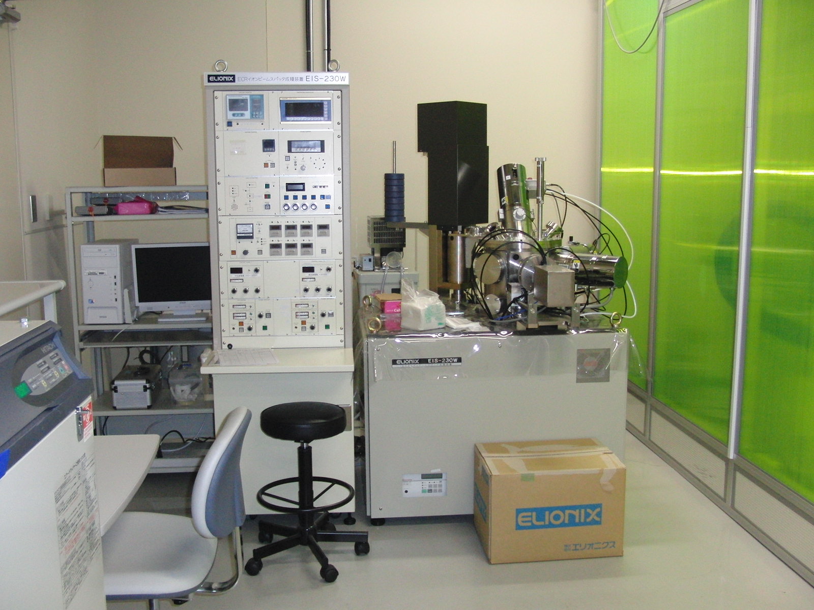
【English】Electron-Cyclotron Resonance (ECR) Ion Beam Sputter Deposition System, EIS-230W
【別名】
【型式番号】EIS-230W (株)エリオニクス
【apparatus ID】
【機器ID】F-UT-110
【機能】イオン銃:スパッタ用2本、アシスト用1本、計3本搭載。多層膜の形成や異種ターゲット構成原子の混ざり合った混合膜の形成が可能。薄膜形成時にイオンビ-ムミキシングや薄膜形成原子の表面での攪拌、結晶化の促進等が可能。(詳細)
【Alias】Electron-Cyclotron Resonance (ECR) Ion Beam Sputter Deposition System
【Model Number】EIS-230W (Elionix inc.)
【Apparatus ID】
【Equipment ID】F-UT-110
【Specifications】 Three ion guns are installed. Two for sputtering and one for assist. It can deposit multi-layer and mixed thin-films. Ion beam mixing, mixing of constituent atoms at the surface of thin-films and enhancement of crystallization are available, when depositing. (detail)
CVD(化学気相成長)、有機膜
CVD (Chemical Vapor Deposition), Organic film
CVD(Chemical Vapor Deposition:化学気相堆積)法は原料をガスや蒸気にして、加熱した半導体の基板上に化学反応により結晶や非晶質を堆積する方法。原料物質を含むガスに、熱や光によってエネルギーを与えたり、高周波でプラズマ化したりすることにより、原料物質をラジカル化して化学反応を活性化している。
CVD (Chemical Vapor Deposition) is a method of depositing crystals or amorphous materials by chemical reaction on a heated semiconductor substrate using raw materials as gas or vapor. The gas containing the raw material is energized by heat or light, or plasmaized by high frequency, to radicalize the raw material and activate the chemical reaction.
パリレンコーター
Parylene coater
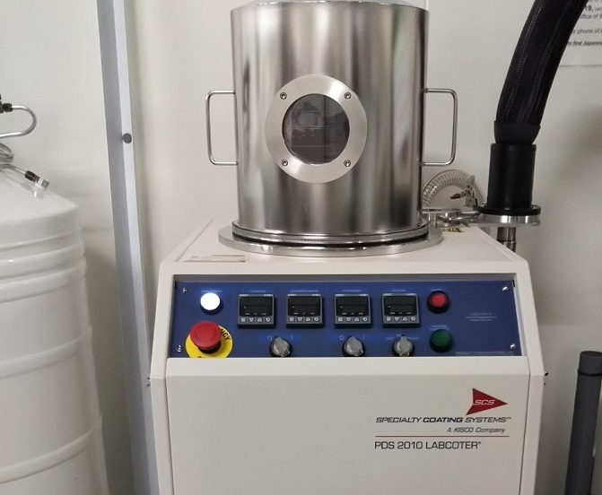
【English】Parylene coater SCS PDS2010
【別名】
【型式番号】米国SCS社製 PDS2010
【apparatus ID】172
【機器ID】F-UT-147
【機能】8インチまでの成膜が可能。
【Alias】Parylene coater SCS PDS2010
【Model Number】PDS2010 manufactured by SCS, USA
【Apparatus ID】172
【Equipment ID】F-UT-147
【Specifications】PDS 2010 LABCOTER 2
Maximum sample size: 8''.
めっき
Plating
めっき(plating)は、金属などの材料の表面に、金属の薄膜を被覆する表面処理をいう。一般には電解液で電流を流してカソード電極となる材料表面に金属を析出させる。また、電流を流さず、化学反応により金属を析出する無電解めっきがあり、この場合は対象物は金属に限らない。
Plating is a surface treatment that coats the surface of a material, such as a metal, with a thin film of the metal. Generally, an electric current is passed through an electrolytic solution to deposit the metal on the surface of the material that serves as the cathode electrode. There is also electroless plating in which no current is applied and the metal is deposited by a chemical reaction, in which case the object is not limited to metal.
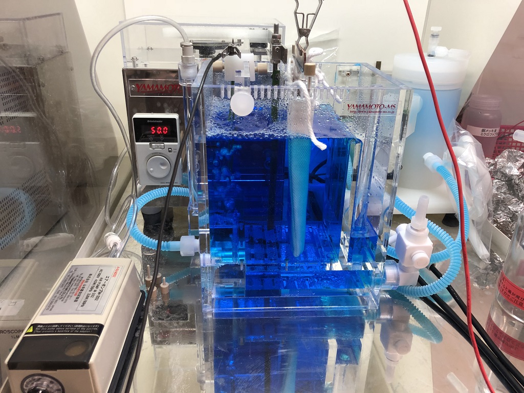
金メッキ装置
Gold electroplating apparatus
【English】Gold electroplating apparatus
【別名】
【型式番号】山本鍍金試験器製
【apparatus ID】157
【機器ID】F-UT-135
【機能】欠片~4”までの金電解メッキ
【Alias】
【Model Number】From Yamamoto-ms company
【Apparatus ID】157
【Equipment ID】F-UT-135
【Specifications】Maximum sample size: 4''. Electrolytic gold plating.
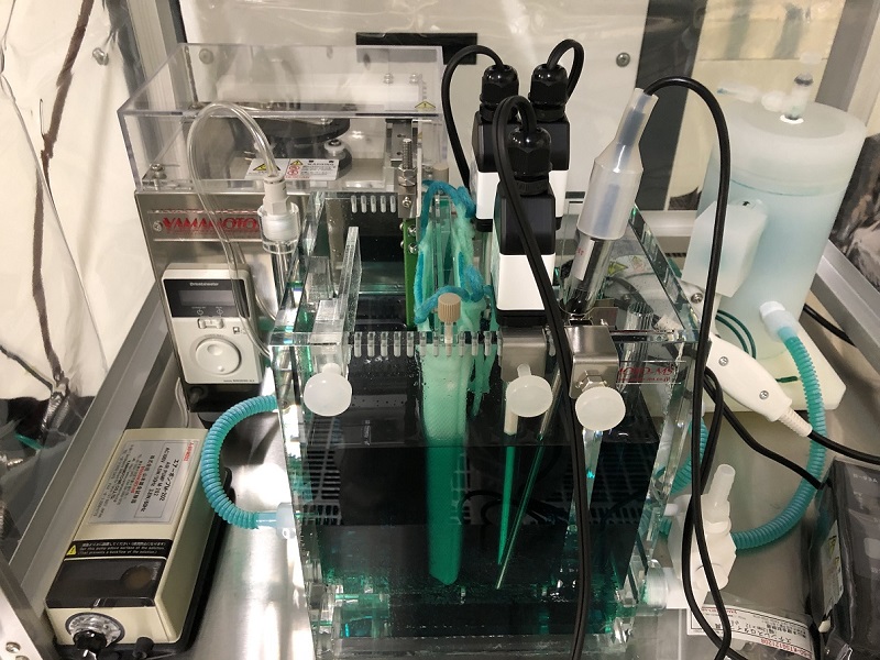
銅メッキ装置
Copper electroplating apparatus
【English】Copper electroplating apparatus
【別名】
【型式番号】山本鍍金試験器製
【apparatus ID】158
【機器ID】F-UT-136
【機能】欠片~4”までの銅電解メッキ
【Alias】
【Model Number】From Yamamoto-ms company
【Apparatus ID】158
【Equipment ID】F-UT-136
【Specifications】Maximum sample size: 4''. Electrolytic copper plating.
超臨界銅成膜装置
Supercritical Fluid (SCF) Deposition
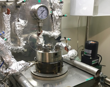
【English】Supercritical Flude (SCF) Deposition
【別名】
【型式番号】
【apparatus ID】
【機器ID】F-UT-140
【機能】自作2㎝角まで。東京大学霜垣・百瀬研究室との協力による。
【Alias】
【Model Number】
【Apparatus ID】
【Equipment ID】F-UT-140
【Specifications】Maximum sample size: 2cm. Developed with the help of Shimogaki-Momose Lab, UTokyo.
ニッケルめっき装置
Nikel electroplating apparatus
【English】Nikkel electroplating apparatus
【別名】
【型式番号】山本鍍金試験器製
【apparatus ID】171
【機器ID】F-UT-148
【機能】欠片~4”までのニッケル電解メッキ
【Alias】
【Model Number】From Yamamoto-ms company
【Apparatus ID】171
【Equipment ID】F-UT-148
【Specifications】 Maximum sample size: 4''. Electrolytic nickel plating.